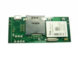

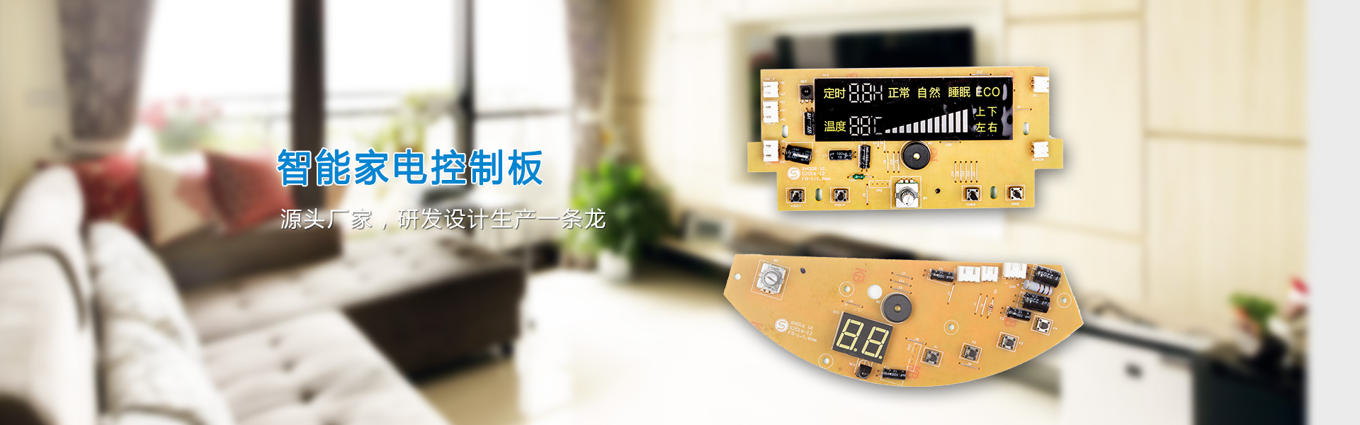


LCD test board PCB circuit board main characteristics of circuit board scheme design, development and production1. Power input: 12V input is recommended, ranging from + 7V to 15V;2. Working temperatur
2021-11-26 admin 96
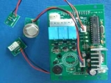
Technical parameters of spraying machine control board development and R & D scheme design companyMaximum output pressure: 0.6 (n / s)Power: 750 (W)Power: 0.83 (W)Processing customization: Yes
2021-11-26 admin 97
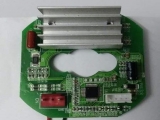
Palm vein recognizer control board development and R & D scheme design company's technical parametersProcessing customization: YesMechanical rigidity: rigidityNumber of layers: double and
2021-11-26 admin 156
The main reasons for the failure of PCBA processing solder joints:1. Poor component pins: plating, pollution, oxidation, coplanarity;2. Bad PCB pads: plating, pollution, oxidation, warpage;3. Solder q
2020-12-28 admin 134